(TBench) 2.3 Extract Signal Names and setup the Clock |

|

|
|
(TBench) 2.3 Extract Signal Names and setup the Clock |
|
|
(TBench) 2.3 Extract Signal Names and setup the Clock |
|
|
|
(TBench) 2.3 Extract Signal Names and setup the Clock |
|
|
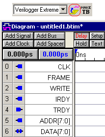
Next we will extract the signal names, types, and size from the port information contained in the mymut.v file.
Extract MUT ports into Diagram
•Press the Extract MUT ports into Diagram button on the main window button bar to extract the top level ports from mymut.v and dump them into a timing diagram window. Notice that these ports match the signals in the mymut.v code |
|
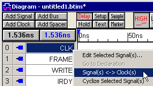
Convert the CLK signal into a SynaptiCAD Clock Signal:
The Extract MUT Ports function imports all the port signals into SynaptiCAD Signals. However, we would like the clock to draw itself based on a frequency. To do this we need to covert the CLK signal into a CLK clock.
•Right-click on the CLK label name and select Signal <-> Clock from the context menu. This will convert the signal to a clock, and draw a clock waveform with a default frequency of 10MHz. •The default clock values are fine for this tutorial, but if you want to look at the Clock Properties, double click on the clock waveform to open the Edit Clock Parameters dialog. Close it when you are done. |
|
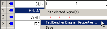
Set the default Clock Signal to make a cycle based test bench
Next set the Clock signal and Edge for all of the signals in the diagram so that the test bench will be cycle-based instead of time-based (this means the test bench stimulus will change after waiting on clock transitions instead of time delays).
•Right-click on a signal name and select TestBencher Diagram Properties context menu to open a dialog of the same name. |
|
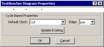
•In the Default Clock drop down, select CLK as the default clocking signal to use and set the Edge dropdown as pos to specify positive-edge clocking. •Click the Update Existing button to set the clocking signal for existing signals. Press OK to close the dialog. |
|
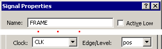
•That dialog set the clock signal for every normal signal in the diagram. This could have been done individually by double clicking on each signal name to open the Signal Properties dialog and setting the controls there. The individual settings are used when you have multiple clocking domains. |
|
Examine the difference between a cycle-based and time-based test bench:
Following is a code example of the difference between a cycle-based and time-based test bench. Both of these code segments were exported from the diagram you will be drawing in the next step. Signals with the same clocking signal and edge type will be driven by a common process in the generated code. We call a process of this type a Clocked Sequence. All the unclocked signals are driven by the Unclocked Sequence. This means that when a diagram contains signals with different clocking signals, a separate sequence process will be created for each clocking signal/edge type. Clocked Sequences are named based on the clocking signal and the edge type, so for this example, the clocked sequence that contains the code on the right will be called CLK_pos.
Time Based Code |
Cycle-based Code |
#137; FRAME_driver <= 1'b0 #3; WRITE_driver <= 1'b0 ADDR_driver <= 8'h00 #100; WRITE_driver <= 1'b1 IRDY_driver <= 1'b0; ADDR_driver <= 8'hxx DATA_driver <= 8'hAA #100; FRAME_driver <= 1'b1 IRDY_driver <= 1'b1; DATA_driver <= 8'hzz #101; |
repeat (2) begin @(posedge CLK); end FRAME_driver <= 1'b0;
WRITE_driver <= 1'b0; ADDR_driver <= 8'h00; @(posedge CLK); WRITE_driver <= 1'b1; IRDY_driver <= 1'b0; ADDR_driver <= 8'hxx; DATA_driver <= 8'hAA; @(posedge CLK); FRAME_driver <= 1'b1; IRDY_driver <= 1'b1; DATA_driver <= 8'hzz; @(posedge CLK); |