(TBench) 3.5 Create the Write Cycle Transaction Diagram |

|

|
|
(TBench) 3.5 Create the Write Cycle Transaction Diagram |
|
|
(TBench) 3.5 Create the Write Cycle Transaction Diagram |
|
|
|
(TBench) 3.5 Create the Write Cycle Transaction Diagram |
|
|
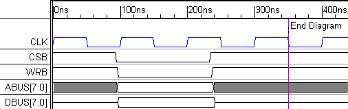
TestBencher Pro uses timing diagrams to represent reusable bus transactions. This tutorial will use two timing diagrams, tbread.btim and tbwrite.btim, to represent the read and write cycles used in testing the memory module. First, draw the write cycle diagram and then create variables for the data and address busses so that new values can be passed to the timing diagram each time it is called by the sequencer. Variables are also used to provide comparison values for runtime testing, and this will be demonstrated in the read diagram.
Create the Write diagram from the Template:
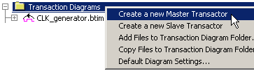
•In the Project window, right click the Transaction Diagrams folder and select Create a new Master Transactor from the context menu. This will cause the Save As dialog to open. |
|
•Name the file tbwrite and press the Save button. This creates a new timing diagram using the information in the template file and lists the file in the Transaction Diagram folder. |
|
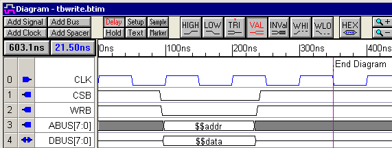
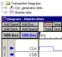
Draw the waveforms for the Write diagram:
Sketch the waveforms as shown on the diagram below. Since this is a negative edge clocked diagram the exact placement of signal edges is not important (unless it is near a negative clock edge). If you need a help drawing, refer to the Basic Drawing and Timing Analysis Tutorial sections 1.2 Drawing Signal Waveforms.
Add the variables:
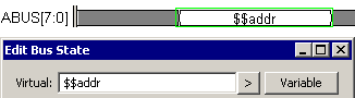
•Double click on the valid segment in the center of ABUS to open the Edit Bus State dialog. |
|
•Type $$addr into the Virtual edit box. The "$$" in front of the variable name indicates that this is a state variable. If the "$$" is missing, TestBencher Pro will assume that this is the value of the address rather than a variable that will accept a value at a later time. |
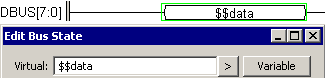
•Click on the valid segment in the center of DBUS to move the focus of the Edit Bus State dialog to the new segment. |
|
•Type $$data in the Virtual edit box, then press the OK button to close the Edit Bus State dialog. The two edited segments will display the state variables. •Click the diskette icon |
Below is the completed write transaction. When the chip select (CSB) and the write enable (WRB) are low, the address and data busses will be driven with the current values of the $$addr and $$data variables.