(TD) 6.13 Verify the Histogram Circuit |

|

|
|
(TD) 6.13 Verify the Histogram Circuit |
|
|
(TD) 6.13 Verify the Histogram Circuit |
|
|
|
(TD) 6.13 Verify the Histogram Circuit |
|
|
At this point we have modeled the entire histogram circuit, so your diagram should resemble the figure below. If it doesn’t, check the simulation.log for errors and correct as necessary. The output of the $display commands will be particularly useful if you are getting x’s on your DBUS signal which indicates unknown data is being read from your RAMs. One thing to check for is that your diagram is never performing a write to an unknown address (an address containing x's) in your RAM bank. If you write a value to an unknown address, the memory model has no way of knowing which memory location has been changed. Therefore, all the memory locations in the entire address space of the RAM bank may or may not have been changed. The memory model is forced to represent this unknown state by setting all memory locations in the SRAM to x!
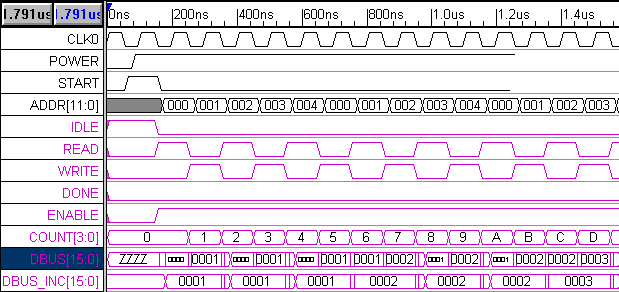
Figure 3: Completed Timing Diagram