(TD) 2.4 Register and Latch Signals |

|

|
|
(TD) 2.4 Register and Latch Signals |
|
|
(TD) 2.4 Register and Latch Signals |
|
|
|
(TD) 2.4 Register and Latch Signals |
|
|
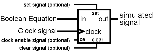
The Interactive Simulator can register or latch the result of a Boolean equation. This circuit is similar to most FPGA cells and can model a large number of components. Below is a figure of the register that a Simulated Signal models. If no clocking signal is chosen, then the Boolean equation goes straight to the signal output as shown in the previous sections. Note: setting the MSB/LSB fields in the Signal Properties dialog will "parallelize" the circuit, allowing multi-bit registers such as counters, shifters, etc. to be modeled.
Experiment with the register and latch equations:
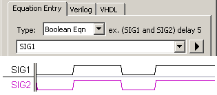
•Change the SIG2 equation to just one term SIG1 and press the Simulate Once button. SIG2 should be an exact copy of SIG1.When we register SIG2 you can visually compare it to SIG1 to see the effects of the register. |
|
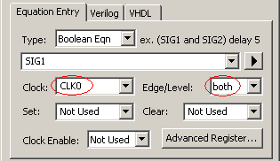
•Set the clock control to CLK0. Choosing a clock brings in the register/latch model to buffer the Boolean equation. •Set the edge/level control to both, to indicate that both the rising and falling edges of the clock are triggering edges. Since it is edge triggered a register circuit will be created rather than a level sensitive latch. |
|
•Click the Simulate Once button to simulate the circuit. Notice that SIG2 only transitions when CLK0 has a positive or negative edge transition (move some edges on SIG1 to verify this). |
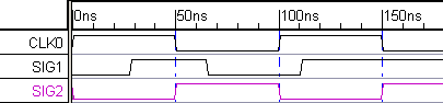
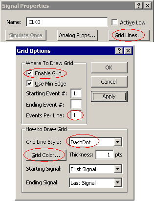
•To make the diagram look like the above picture, we hid SIG0 because it is not being used. •We also added Grid Lines to every edge of the clock. To do that double click on the clock name to open the Signal Properties dialog and press the Grid Lines button. This opens the Grid Options dialog. Play with the controls and hit Apply until you get an image that you like. |
|