|
|||||||||||||||||||||||||||||||||||||||||||||||||||||||||||||||||||||||||||||||||||||||||||||||||||||
|
|
Simulated SignalsWaveFormer Pro, DataSheetPro, VeriLogger and TestBencher Pro have a built-in Interactive HDL Simulator that greatly reduces the amount of time needed to draw and update a timing diagram. Using Boolean and Registered logic equations written in VHDL, Verilog, or SynaptiCAD's syntax you can describe signals in terms of other signals in the diagram. You will no longer have to figure the output of a combinational circuit or calculate the critical path of a synchronous circuit by hand. SynaptiCAD's interactive simulator will generate the HDL code using information entered into the Logic Wizard dialog and then simulate the result. And since the simulator is interactive, changes to input waveforms will automatically re-simulate so that your timing diagrams always reflect accurate design data. This feature is included in the VeriLogger and TestBencher products even though they have a built in Verilog simulator, because it makes generating test benches and timing diagrams so fast that we couldn't hold it back. In WaveFormer, it is the backbone of the timing analysis and design features. The Interactive simulator supports multi-bit equations and true min-max timing. Below are some examples of equations that are supported.
Boolean EquationsBoolean equations combinationally relate one signal to other signals in the diagram. The equations are entered into the Signal Properties dialog using VHDL, Verilog, or SynaptiCAD's enhanced equation syntax. The SynaptiCAD format supports a special delay operator that takes a signal on the left and time or parameter name on the right and returns a signal. If a parameter name is used on the right hand side of the delay operator, then the equation will simulate true min/max timing. This true min/max timing is the main advantage that SynaptiCAD's format has over the VHDL or Verilog format. Also, by changing a diagram level setting, the simulator will perform min-only or max-only simulations instead of the default min/max simulations. Below are some example Boolean equations using SynaptiCAD's syntax:
Multiplexers and Tristate GatesThe equation box accepts C language conditional expressions in the form of conditional ? if_expr : else_expr . These expressions are useful for modeling multiplexers, tristate gates, and more complicated sequential circuits such as counters. Some examples are:
Multi-bit EquationsMulti-bit Equations are specified by setting the MSB and LSB of the signal (located at the bottom of the Signal Properties dialog). To change a simple 1-bit equation to a 4-bit equation, all you have to do is set the MSB of the signal involved to 3. All register and latch operations support multi-bit signals. Signal ConcatenationConcatenation of Signals is supported using the Verilog concatenation operator. You must set the MSB in the Signal Properties dialog to the proper size. If the size of the concatenated signal is larger than the receiving signal, then the most significant bits are dropped. Some examples of the concatenation operator:
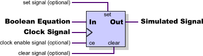
Register and Latch SettingsThe interactive sumulator supports registered and latched equations. Below is an example of the circuit that is being modeled.
The logic wizard in the Signal Properties dialog is used to enter information about the circuit. To use a register or latch just enter a Boolean equation, a clocking signal, and choose the triggering for the clock signal (rising edge, falling edge, both, high, or low). Other settings can be used to describe the control lines for the flip-flop like the clock enable, set and clear signals. These control lines can be active low or high and synchronous or asynchronous depending on the settings in the Advanced Register and Latch Controls dialog (see next bullet).
Timing settings support clock to output delay, input setup time, and output hold time. |
|
|