|
|||||||||||||||||||||||||||||||||||||||||||||||||||||||||||||||||||||||||||||||||||||||||||||||||||||
|
|
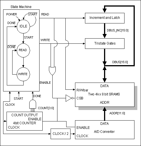
Tutorial 6: Advanced Modeling and SimulationThis tutorial demonstrates how WaveFormer Pro can quickly model and simulate a digital system of moderate complexity. We will be modeling a circuit that computes histograms for 64K of data generated by a 12-bit Analog-To-Digital converter (this is a popular method for testing dynamic SNR for ADCs). This circuit is a simplified form of a real VME board that would take several months to model and simulate using conventional EDA tools. Using WaveFormer, we will model and simulate this simplified circuit in 20 minutes. The full circuit with the complete VME bus interface protocol could be modeled and debugged in about 4 hours. Note: WaveFormer Pro simulation uses Verilog code. This tutorial uses Verilog to code to simulate waveforms and also uses an operator that is Verilog specific. For this reason, this tutorial should be performed in Verilog. VHDL users will find the information useful and will also gain a better understanding of the tool.
Figure 1: Histogram circuit block diagram. This tutorial teaches the user how to:
Before you begin the tutorial you may wish to view Figure 3 in Section 13 which shows a completed version of the diagram that we will generate. File tutsim.tim included in the product directory is a finished tutorial file. You will not use this file during the tutorial itself, but you can always refer back to this file if you encounter any problems during the tutorial. Circuit OperationA histogram is a graph displaying the count of same 12-bit values received from the ADC. To store the histogram count values we will use a 4K SRAM (212 storage cells) to hold a count for each possible 12-bit value that the ADC can generate. The width of the SRAM depends on how many data values we will accumulate from the ADC. In the worst case, the ADC could generate the same value for the entire histogram accumulation, so the SRAM must be able to store a value of up to 4K. Thus we will use 2 8-bit wide SRAMs (216 = 64K > 4K). When the circuit starts operation, the SRAM should contain zeros at every address. Each time a data value is generated by the ADC, that data value is used as an address to look up the current count for the data value in the SRAM. The count is incremented by one and the new value is written back to the SRAM. This continues until the circuit has received 4K data values. 1. Set up a new timing diagramCreate a new timing diagram to model the histogram circuit:
Now that we have a new diagram to work with, we are ready to model the components of our circuit. 2. Generate the Clock, Draw Waveforms, and Use Waveform EquationsThe histogram circuit has a system clock, CLK0, and three signal inputs, POWER, START and ADDR. We will create the waveforms for each of these signals using three different methods: generating from clock parameters, drawing waveforms by hand, and automatically generating waveforms from temporal equations. 2.1 Automatically generate the CLK0 system clock Clocks are repetitive signals that draw themselves based on their attributes: period or frequency, duty cycle, edge jitter, offset and other parameters. Add a clock named CLK0 with a period of 100 ns:
Note: Clocks can also be related to other clocks by using formulas that reference another clock's attributes like period, offset, and jitter. For more information on modeling complex clocks read Chapter 2 in the on-line help. 2.2 Graphically draw the POWER and START signal The POWER signal is a power-on reset signal that we will use to set the initial state of our state machine. The START signal is an external input to the system that pulses high to initiate acquisition in the histogram circuit. The POWER and START waveforms are relatively simple, so we will draw them with the mouse. First add a signal and name it POWER:
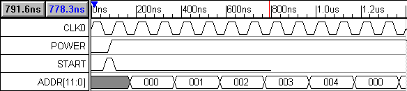
Next, draw the POWER signal so that it is low for 80ns, then high for 2000ns:
Now, add the START signal.
Next, draw the START signal so that it is low for 60ns, high for 100ns, and then low for 800ns:
Waveform drawing and editing techniques can be found in Chapter 1: Signals and Waveforms in the online help. 2.3 Use Temporal and Label Equations to model ADDR (A/D converter's output data) We will model the A/D converter just as a data source, so all we need to do is generate a virtual bus signal called ADDR (the output from the ADC) that drives the address lines of the SRAMs. The ADDR waveform has a regular pattern that can be described easily using an equation, but would be tedious to draw by hand. Add a virtual bus signal called ADDR:
The A/D converter is driven by a clock that is ½ the frequency of the state machine clock CLK0, so the ADDR value should change every other clock cycle (this maintains the same address for the read out of each RAM cell's count data and its write back after it is incremented). The ADDR signal should be unknown for 170ns then it should have twenty valid states, each 200ns in duration. Use the Waveform Equation interface of the Signal Properties dialog to generate the ADDR waveform:
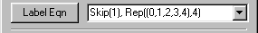
Next, we will label the states of the ADDR bus using a Label Equation. Each state could be labeled individually using the extended state field of the HEX dialog box, but labeling twenty states would take a long time. Instead, we will write an equation to label all the states at once. Chapter 11 covers all the different state labeling functions. To label the equation: In the Signal Properties dialog, enter the equation: Skip(1), Rep( (0,1,2,3,4), 4) in the edit box next to the Label Eqn button. Press the Label Eqn button to apply the equation.
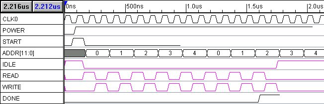
This equation will generate a hex count from 0 to 4, and then repeat it 4 times. The Skip(1) means start labeling after the first state (which we defined to be an invalid state using our waveform equation). Your timing diagram (at the appropriate zoom level) should now resemble the diagram below.
3. Modeling state machines using the Boolean Equation interfaceWe will use a simple one-hot state machine to control the circuit, and we will model the state machine using the Boolean Equation interface. A one-hot state machine uses a single flip-flop for each state. At any given time, only the flip-flop representing the current state will contain a 1, the other flip-flops will be at 0 (hence the name one-hot). One-hot state machines are very popular in FPGA-based designs as they match well with FPGA architectures (they tend to run faster and use less space than traditional Binary Coded state machines in FPGAs).
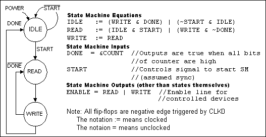
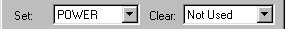
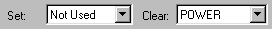
Figure 2: State diagram and design equations for the histogram controller state machine The state machine (SM) initializes to the IDLE state. On the negative edge of the clock after START goes high, the SM will enter the READ state and look up the current count for the current address value being output by the A/D converter. This value will be incremented by a simple fast-increment circuit. On the next clock, the SM will enter the WRITE state, latching the incremented value into a transparent latch called DBUS_INC and initiating the write back of the incremented data to the SRAM. The state machine will continue to toggle between the READ and WRITE state until the desired number of data values have been histogrammed (determined by the size of the binary counter called COUNT), at which point the SM will return to the IDLE state. Figure 2 shows the SM that we will model. The state machine is modeled in WaveFormer using the Boolean Equation section in the Signal Properties dialog (one signal for each state). Next we will enter the equations for the state machine, however these signals are not simulated until Section 5 because signal DONE has not yet been defined. Create three signals called IDLE, READ, and WRITE (one for each flip-flop):
For each signal, perform the following steps in the Signal Properties dialog box:
IDLE := (WRITE & DONE) | (~START & IDLE) READ := (IDLE & START) | (WRITE & ~DONE) WRITE := READ
Notice the
4. Checking for Simulation Errors
The status bar in the lower right corner displays success/failure information about the last interactive
simulation. Currently the corner status bar displays
When your simulation fails, there are two different files you can check to find out why the simulation failed. The first place is in the waveperl.log file which helps you locate syntax errors and undefined signal name errors made in the Boolean Equation edit box. The second place is the verilog.log file which helps locate HDL coding errors in the behavioral code that you type into WaveFormer or external models that you include in the simulation. When you are using just the Boolean Equation interface (like right now) most errors will be simple syntax errors and undefined signal names so the waveperl.log file is a faster way to find the error. For the sake of the tutorial we will examine both files. 4.1 Check the waveperl.log file for equation syntax errors: The file verilog.log contains a status report from WaveFormer about converting your flip-flop equations to Verilog code. This file will show syntax errors and unknown signal names in your design equations.
- Double click on the signal name READ and press the Simulate Once button
- To view the verilog.log file in the Report window: click on the verilog.log tab
4.2 Check the Simulation Log File verilog.log for HDL coding errors If you check the simulator log file, verilog.log in the Report window, you will see an error message reporting that DONE is not declared. The log file also reports the lines in the WaveFormer-generated Verilog source code file where this error occurred. The WaveFormer-generated source file will have the same filename as your diagram, but with a file extension of .v instead of .tim (so if your diagram is untitled.tim, the source code file is untitled.v). This source file is automatically opened by the Report window whenever WaveFormer Pro generates this file (by default this occurs every time you make a change to your design while simulating signals). View the HDL lines where the errors occur:
NOTE: Do not make changes in this source file as your changes will automatically be overwritten the next time a simulation is performed; instead, we will make the appropriate changes in the Diagram window and Signal Properties dialog. Then your product will generate and simulate a corrected file. 5. Simulating Incrementally by temporarily modeling outputs as inputsOne common problem in simulating and debugging digital systems is that large parts of the design have to be entered before testing can begin because the parts provide input to each other. One solution is to break a design up into pieces and test each piece with test vectors that represent the output of the other pieces. However, generation of the test vectors can be time consuming. SynaptiCAD products provide a very simple and quick method for testing small parts of a design: graphically draw the signals for the missing parts of the design to test the design at its current state of development. Then later add the design information that models these signals (in other words, we temporarily model simulated outputs as drawn inputs). We will now use this method below to verify the operation of our state machine before we enter the HDL code that generates the DONE signal:
Make sure everything is working properly:
Once you have the circuit simulating properly, let’s see what happens if the START pulse gets too small:
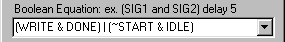
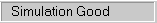
6. Modeling Combinatorial LogicIn addition to the state signals, the state machine has one other output signal called ENABLE that is used to enable the SRAM, the DONE counter, and the ADC. ENABLE is just the output of an OR gate with the READ and WRITE signals as inputs. In Section 3 we used the Boolean Equation interface to model the flip-flops of the state machine. We will use the same interface to model combinatorial logic. To do this choose the default clock called unclocked. If a signal other then unclocked is selected, then the Boolean Equation interface models registers or latches depending on the type of Edge/Level trigger selected. Chapter 12 covers the advanced features of the Boolean Equation interface including the min/max delay features. Model the Enable logic:
7. Entering direct HDL code for simulated signalsFor simplicity, the counter output COUNT is modeled using a simple block of behavioral HDL Code instead of using Boolean equations. It would take a large number of Boolean equations to model the counter and the equations would be difficult to modify if the counter operation had to be changed. For this tutorial we will create a 4-bit counter to test our system. This counter could be easily modified later to make it 12-bit (to acquire 4K worth of data). To enter direct HDL code for the COUNT signal:
Verilog Note: All signals in WaveFormer are modeled as wires, so the assign is required at the end of the HDL code block to drive the COUNT wire with the value of COUNTER (which must be a register in order to remember its value). To increase the size of the counter to acquire 4K data values (do not do this now), we could change the MSB of COUNT to 11 and change the declaration of COUNTER in the HDL code to: reg [11:0] COUNTER; //example only, don't
do in this tutorial
8. Modeling n-bit gates Using a Reduction-AND operator-- Modeling the DONE signalNext we will model the DONE signal that we originally drew as an input to the state machine. The DONE signal is generated by performing a bitwise AND of the COUNT signal (we are done whenever all the counter bits are high). To model the DONE Signal:
The & operator when used as a unary operator is called a reduction-AND operation. A reduction-AND indicates that all the bits of the input signal should be ANDed together to generate a single bit output. This is equivalent to the following equation: COUNT[0] & COUNT[1] & COUNT[2] & ... One nice benefit of using a reduction operator instead of the above equation is that it automatically scales the circuit to match the current size of the COUNT signal (it’s also a lot easier to type)! 9. Incorporating pre-written HDL models into WaveFormer simulations-- Modeling the SRAMWe will use an SRAM HDL module contained in an external file (sram.v) to model the SRAM. This model is fairly complex and accurately models the asynchronous interface that is commonly used by most off-the-shelf SRAMs. One special feature is that the SRAM resets all its memory cells to zero when it first starts up. In a real circuit, we would need to add extra logic to iterate through the addresses, writing zeros at each one. A full description of the Verilog modeling of this SRAM is outside the scope of this tutorial, but let’s take a quick look at it inside the Report window:
9.1 Including an external SRAM Verilog model file into WaveFormer To add the SRAM model to our design we need to modify the wavelib.v file that contains the models used by WaveFormer. The SRAM model code cannot be entered into a signal’s HDL code window because the model declares a module and modules cannot be nested in Verilog (WaveFormer puts all the HDL code from signals into a single module called testbed). All user-written Verilog modules should be declared in wavelib.v (or preferably, included from separate files into wavelib.v using the include directive as will be doing). In this case, the source code for the SRAM is already contained in a separate file called sram.v and we only need to add an include statement to wavelib.v to let WaveFormer know about it. To modify the wavelib.v file: - Select the menu option Report > Open Report Tab and open the wavelib.v file. - Add the following line to the beginning of the wavelib.v (it may already be there depending on which SynaptiCAD product you are using): `include "sram.v" - Select the Report > Save Report Tab menu option to save your change. 9.2 Instantiating the SRAM component models To drive the data bus DBUS, we need to instantiate two instances of the SRAM model:
wire CSB = !ENABLE;
sram BinMem1(CSB,READ,ADDR,DBUS[7:0]);
sram BinMem2(CSB,READ,ADDR,DBUS[15:8]);
The first line creates an internal signal that is an inverted version of the ENABLE line (the SRAM is active low enabled). The next two lines instantiate two 4Kx8 SRAMs and connect up their inputs and outputs (the first SRAM contains the low byte of the count and the second contains the high byte). 10. Modeling the Incrementor and Latch circuitIn Section 3 we used the Boolean Equation interface to model the state machine using negative edge-triggered registers. Now we will use the same interface to generate level-triggered latches used to model the increment-and-latch circuit. The value stored in the SRAMs is placed on DBUS and the incrementor circuit takes that value, adds one to it, and latches the incremented value:

11. Modeling tri-state gates using the conditional operatorThere are 2 possible drivers for DBUS: the SRAMS which we modeled in section 9, and the tri-stated output of the DBUS_INC signal. All the drivers for a bus should be included in the code for the bus. To add the tri-state gate to DBUS:
assign DBUS = WRITE ? DBUS_INC : 'hz;
Line 4 models the tri-state gates that follow the latches in the histogram circuit. These tri-state gates are enabled whenever the WRITE signal is high. We use the conditional operator (condition ? x : y) which acts like an if-then-else statement (if condition then x else y). If WRITE is high, DBUS is driven by DBUS_INC (the incremented version of DBUS that we latched), else the tri-state drivers are disabled (‘hz means all bits are tri-stated). 12. Using $display and $monitor statements to debug external Verilog modelsVerilog contains two system tasks (commands), $display and $monitor, that can be included in Verilog source files for debugging purposes. $display acts like a C-language printf statement which prints to the simulation log file verilog.log whenever it is executed by the Verilog simulator. $monitor is similar, but it automatically prints to the log file whenever any of the signals listed in this command change state. The SRAM model file sram.v contains two $display statements that output the address and data values for the SRAM whenever the SRAM is read from or written to (you can view the $display commands in sram.v in the Report window). You can see the output of the $display commands by viewing verilog.log in the Report window. 13. Verify the Histogram CircuitAt this point we have modeled the entire histogram circuit, so your diagram should resemble the figure below. If it doesn’t, check the verilog.log for errors and correct as necessary. The output of the $display commands will be particularly useful if you are getting x’s on your DBUS signal which indicates unknown data is being read from your RAMs. One thing to check for is that your diagram is never performing a write to an unknown address (an address containing x's) in your RAM bank. If you write a value to an unknown address, the memory model has no way of knowing which memory location has been changed. Therefore, all the memory locations in the entire address space of the RAM bank may or may not have been changed. The memory model is forced to represent this unknown state by setting all memory locations in the SRAM to x!
Figure 3: Completed Timing Diagram14. Using an End Diagram Marker to control the length of the simulationBy default, WaveFormer simulates to the last drawn signal edge. You can also use a time marker to control the length of the simulation. To place a time marker:
15. Editing Verilog source files inside WaveFormerTo demonstrate how to make changes to a Verilog source file inside WaveFormer, we will edit the SRAM model file sram.v in the Report window:
You may have anticipated that DBUS would now show 8 (we did when we first did this tutorial!), but it is correct in showing 808 because our DBUS is a 16-bit value composed of the data in two parallel SRAMs each initialized with 08 (hence 0808 = 808). 16. Simulating your model with traditional Verilog simulatorsThe verilog model of your system created by WaveFormer can also be simulated by traditional Verilog simulators. The complete verilog model simulated by WaveFormer is composed of (1) the verilog file generated by WaveFormer (untitled.v for this tutorial), (2) the WaveFormer library file wavelib.v, and (3) any external model files you have included (e.g. sram.v for this tutorial). Follow the instructions of your Verilog simulator to simulate these files together. SummaryThis concludes the advanced simulation tutorial. Other simulation features not covered in this tutorial that you may wish to experiment with are: flip-flop timing characteristics (clock to output propagation delay and continuous setup and hold time checking) in the Signal Properties Dialog and the global simulation options in the Options\Simulation Preferences Dialog. |
 to open the Edit Clock Parameters dialog.
 . This
adds a signal called SIG0.
. This
adds a signal called SIG0. on the button bar to activate it. The next waveform segment will be drawn low.
 Changing the MSB and Radix defines ADDR as a 12-bit signal that display its values in hexadecimal
format.
Changing the MSB and Radix defines ADDR as a 12-bit signal that display its values in hexadecimal
format.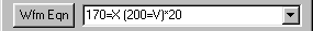
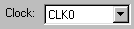 . This sets
the flip-flop to be clocked by CLK0.
. This sets
the flip-flop to be clocked by CLK0.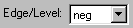 . This
indicates that negative edge triggered flip-flops will be used to model the state-machine. Read Chapter
12 for more information.
. This
indicates that negative edge triggered flip-flops will be used to model the state-machine. Read Chapter
12 for more information. . This
radio button causes an instant resimulation when a change is made in your diagram.
. This
radio button causes an instant resimulation when a change is made in your diagram. display in the bottom right hand corner and notice that the state machine signal names turned gray.
This is because the IDLE and READ equations reference a signal called DONE. This signal has not been
defined so if you try to simulate you get errors. In the next section we will investigate the different
ways to detect and fix simulation errors.
display in the bottom right hand corner and notice that the state machine signal names turned gray.
This is because the IDLE and READ equations reference a signal called DONE. This signal has not been
defined so if you try to simulate you get errors. In the next section we will investigate the different
ways to detect and fix simulation errors. in the Signal Properties dialog (this will generate a warning that we can view in the step below).
 at the bottom of the Report window. In this particular case, varilog.log reports a warning
that the signal DONE has not yet been defined in WaveFormer:
at the bottom of the Report window. In this particular case, varilog.log reports a warning
that the signal DONE has not yet been defined in WaveFormer: 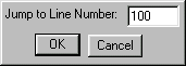
 . If the
indicators still show an error, then the waveperl.log and verilog.log files will help
you to pinpoint the error in your diagram.
. If the
indicators still show an error, then the waveperl.log and verilog.log files will help
you to pinpoint the error in your diagram.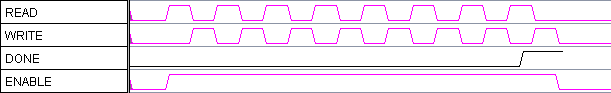
 to switch from the Equation view to the HDL Code view/editor.
 found on the button bar. This turns the Marker button red which indicates that right clicks in the
Diagram window will add marker lines.
found on the button bar. This turns the Marker button red which indicates that right clicks in the
Diagram window will add marker lines.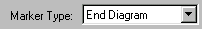 .
.|
|