TestBencher Pro: Performing a Sweep Test
This tutorial will generate a test bench that cycles through read/write transactions on an SRAM model.
It will sweep an input edge to the SRAM model until a setup failure is generated. The SRAM model is
the same model that was used in the TestBencher Basic Tutorial.
This tutorial will demonstrate several advanced capabilities of TestBencher:
-
Create a global clock for a test bench using a concurrent apply call.
-
Generate stimulus vectors as a function of a clocking signal.
-
Use delays to control the timing of an edge transition (making an edge
transition relative to a waveform generated outside a transaction).
-
The use of continuous setups as protocol checkers
-
Place HDL code at the top level to control timing transaction sequencing
and to pass timing values to a transaction at simulation run-time. This allows programmatic and randomized
timing of clocks and edge transitions.
This tutorial picks up where the TestBencher Basic Tutorial left off. Please note that you must have
a full version license or a 30 day evaluation license file to perform the actions in this tutorial.
You can obtain a license file by visiting our website (www.syncad.com/syn_lic.htm) or by contacting our sales department.
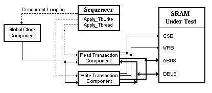
Schematic of circuit that the tutorial test bench will exercise
This tutorial does not cover any of TestBencher Pro’s drawing features or the language independent
bus format. These features are covered in the first five tutorials (Basic Drawing and Timing Analysis,
Interactive HDL Simulation, Waveform Generation and
Bus Tutorial, Advanced Parameter Techniques, and
Advanced HDL Stimulus Generation).
If you are new to SynaptiCAD’s timing
diagram editing environment then you should do the tutorials listed above first. Also, this tutorial will begin with a project that has already been created.
It is assumed that you are able to create TestBencher projects. If you are not familiar with creating
test benches using TestBencher Pro, it is recommended that you perform the TestBencher Basic Tutorial
before completing this tutorial.
This tutorial uses three timing diagrams: tbread.tim (copied from tbread_orig.tim),
tbwrite.tim, and tbglobal_clock.tim
(created during the tutorial). Two versions
of the SRAM sweep test project are provided, named
SweepTest1.hpj and SweepTest2.hpj. The
first version generates a cycle-based test bench, the second generates a timing-based test bench. As
with the TestBencher Basic Tutorial, the only two files in the project that you will need to modify
(aside from the creation of the global clock) are tbread.tim and the top-level template file.
Note: We provide two copies of the read diagram for the possibility of the tutorial being performed
more than once. The file "tbread_orig.tim" contains the diagram in its original state, so
it can be copied and renamed to "tbread.tim".
Preparing your working environment for this tutorial:
If do not have read/write access to the TestBencher Pro installation directory then you must copy the
tutorial files to a new directory to which you have read/write permission. If you can read and write
to the TestBencher Pro directory then skip down to Open the Tutorial Project.
To set up a project directory:
-
Create a new directory or folder called
SweepTest1. This directory should be in a location in your path
to which your account has full read/write access.
-
Copy the following files from the
Examples\Verilog\SweepTest1 or
Examples\VHDL\SweepTest1 directory located in the TestBencher
installation directory into the new SweepTest1
directory:
- SweepTest1.hpj
- tbread.tim
- tbwrite.tim
- tbsram.v or
tbsram.vhd (.v for Verilog
users, .vhd for VHDL users)
-
Copy the following files from the TestBencher installation directory
into the new SweepTest1
directory:
- If you are working with VHDL:
wavelib.vhd and syncad.vhd.
- If you are working with Verilog:
wavelib.v and syncad.v
When the tutorial refers to the SweepTest1
directory, use this new project directory.
ModelSim Integration
If you are going use ModelSim to simulate your projects, you can use the new ModelSim Integration feature
to auto-build the project library and launch the simulator with the design loaded (otherwise, skip ahead
to Open the Project).
As a reminder, TestBencher does provide a Verilog simulator, but the ModelSim Integration can be used
with both dialects of VHDL or Verilog.
To enable ModelSim Integration:
-
Select the Options > External Program Settings
menu option. This will open the External
Program Settings dialog.
-
Check the Enable External Simulator Integration
checkbox. This will disable TestBencher's Verilog simulator and enable the ModelSim Integration feature.
-
Enter the path to the ModelSim executable files
in the Executable Path edit box. This should be the directory that contains the ModelSim executable
files (vlib.exe, vsim.exe,
vcom.exe and vlog.exe).
-
Select the type of operating system that the ModelSim
executable resides on from the Target OS
combo box. This will determine the type of script
that generated to launch ModelSim. When ModelSim is launched using this script the project will be automatically
loaded.
-
If you want TestBencher to automatically launch
ModelSim, check the Launch Simulation on Run
Simulation check box. TestBencher will use
the script described in the previous step to launch ModelSim.
-
Click OK to close the dialog
and enable the ModelSim Integration feature.
Open the Tutorial Project:
-
Select the Project > Open
Project menu option to open the Open Project File
dialog.
-
Move to either the new SweepTest1, Examples\Verilog\SweepTest1 or Examples\VHDL\SweepTest1 directory using the browsing features of the dialog.
-
Select SweepTest1.hpj file name and click the Open File button to load the project into TestBencher. Four files should be displayed
in the Project window: tbread.tim, tbwrite.tim, the tbench1 template file, and the
tbsram model file.
1) Create a Global Clock Generator with Adjustable Period
A global clock generator can be used to synchronize several timing transactions within a test bench.
Typically this is done by using one diagram that runs continuously and concurrently to generate the
clock (the clock signal is an output in this diagram). In the synchronized timing transactions, an input
clock with the same name as the global clock is added to each diagram. Inside the top-level test bench,
TestBencher will automatically connect the global output clock to each of the input clocks. In this
section we will create a timing diagram and add a global clock with an adjustable period. The period
will be specified in the top-level template file later in the tutorial.
1.1 Create a new timing diagram
-
Select the File > New Timing Diagram
menu option. This may cause a dialog to open asking if you want to save the current timing diagram.
If you have made changes that you want to keep, select Yes. Otherwise select No. A new timing diagram now opens in the timing diagram editor.
1.2 Create a Free Parameter to control the clock period
Next, add a free parameter which will become the variable that will allow the clock period to be changed
by the top-level test bench.
-
In the Parameter window, click the
Add Free Parameter button
 . This will add a new free
parameter to the Parameter window. If you do not see the Parameter window, select the
Window > Parameter Window
menu option. . This will add a new free
parameter to the Parameter window. If you do not see the Parameter window, select the
Window > Parameter Window
menu option.
-
Double click on the name of the new free parameter (F0) to open the Free Parameter Properties dialog.
-
Type Period in the Name edit box.
-
Type in the value 100 in the
Min
edit box. The value that you specify for the Min property will have no affect on the
value of the free parameter in the generated testbench for this tutorial. However, it is necessary to
enter a value here so that when we use the free parameter in the clock settings there is something valid
to be evaluated for the period.
-
Check the Is Apply Subroutine Input
checkbox to make this a runtime controllable parameter. This makes the parameter an input to the diagram
call (Apply call) in the top-level test bench. If this checkbox were not checked, then the generated
code would use the min and max values of the parameter.
-
Make sure the Enable HDL Code Generation
checkbox is checked. Without this there will be no HDL code generated for the parameter. This feature
allows you to turn off code generation for the parameter without removing the parameter from the diagram.
-
Click OK to close the
Free Parameter Properties dialog.
1.3 Add a Clock with an adjustable period
Next we will add the global clock. Since this diagram will generate the clock for the entire simulation,
we must make sure that the direction of the clock is output and that the clock is exported from the
timing transaction. We will use the free parameter created above to allow us to set the period of the
clock from the top-level test bench. To add a clock to the diagram and specify the period:
-
Click the Add Clock button
 on the button bar to open the Clock Properties
dialog.
on the button bar to open the Clock Properties
dialog.
-
Type GClock in the Name edit box.
-
Type Period in the Period Formula edit box. This will specify the free parameter that
we just created as the value of the period for the clock. Note that we could also enter an equation
here that included the free parameter as a term, but in this case we just want to perform a direct substitution
of the value of the free parameter.
-
Click OK to close the Clock Properties dialog and add the clock to the diagram.
-
By default, new clocks and signals have a direction of output and have their export signal
check boxes checked. If you want to verify these settings, double click on the clock name to open the
Signal Properties dialog and look at dialog settings.
1.4 Add Global Clock Generator to the Project
-
Right click on clock name to open a pop-up context menu.
-
Select Add Diagram to Project from the menu to open the Save As dialog.
-
Type the name tbglobal_clock.tim in the File name edit box.
-
Click the Save button to save the timing diagram and close the dialog. Notice that the timing
diagram is now a part of the project.
Note: GClock is the only signal
in this diagram. In many instances, this is how you will want the global clock to be incorporated into
your project because you will want the clock to run for the entire duration of the simulation. During
this simulation there are no other processes that will need to run for the entire duration of the simulation.
2) Add Global Clock as an Input to the Read Transaction
Next add the global clock as an input to the read transaction. We will use the global clock to synchronize
the output of stimulus from the read cycle. To add the global clock to the read transaction:
-
In the Project window, double click the
tbread.tim file name to load the timing diagram in the Timing
Diagram Editor window.
-
Click the Add Clock button on the button bar above the signal names in the Timing Diagram
Editor window. This will open the Clock
Properties dialog.
-
Type in the name GClock in the
Name edit box. Note this is the same name as the global clock we defined in the clock
generator diagram (capitalization counts).
-
Click OK to close the
Clock Properties dialog.
-
Double click the name GClock that was just
added to the diagram to open the Signal
Properties dialog.
-
Set the direction to input. Since GClock
is driven by another transaction, the values for GClock will be inputs to this transaction.
-
Click OK to apply the changes
and close the Signal Properties dialog. Notice that the waveform for the clock is
now blue to indicate that its waveform values will be input to the transaction.
3) Change Read Transaction to be Cycle Based
By default, TestBencher will generate time-based transactions which means that an event within a diagram
will generate an event within the HDL code at a specific time relative to the beginning of the transaction.
However when generating test benches for cycle-based simulators the events in a diagram must be synchronized
with a particular clock signal. To change a diagram from time-based to cycle-based, all you have to
do is make the signals reference a clock signal. Below is an example of the unclocked code that is generated
for the read transaction now, and a sample of the cycle-based code that will be generated once you perform
the steps in this section.
Verilog - Unclocked Code Sample
#100       //AbsoluteTime 110
ABUS = addr;
#120       //AbsoluteTime 210
ABUS = 8'bxxxxxxxx;
Verilog - Same edge transitions, off pos edge of GClock:
@ (posedge GClock)
#10.001              //AbsoluteTime 110
ABUS = addr;
@ (posedge GClock)
#10.001              //AbsoluteTime 210
ABUS = 8'bxxxxxxxx;
VHDL - Unclocked Code Sample
wait until (tb_status = DONE) for 110 ns; --AbsoluteTime 110 ns
if (tb_status = DONE) then exit; end if;
ABUS <= addr;
DBUS <= "ZZZZZZZZ";
wait until (tb_status = DONE) for 100 ns; --AbsoluteTime 210 ns
if (tb_status = DONE) then exit; end if;
CSB_Unclocked <= '1';
ABUS <= "XXXXXXXX";
VHDL - Same edge transitions, off pos edge of GClock:
posEdge(tb_status, GClock);
wait until (tb_status = DONE) for 10.001 ns; --AbsoluteTime 110 ns
if (tb_status = DONE) then exit; end if;
ABUS <= addr;
DBUS <= "ZZZZZZZZ";
posEdge(tb_status, GClock);
wait until (tb_status = DONE) for 10.001 ns; --AbsoluteTime 210 ns
if (tb_status = DONE) then exit; end if;
CSB_GClock_pos <= '1';
ABUS <= "XXXXXXXX";
Set the Clock property of each
Signal to indicate Cycle-based code generation:
-
Select CSB, WRB, ABUS and DBUS
at the same time. You can do this by either clicking each individual signal name or by clicking the
top signal name and dragging across the other signal names.
-
Right click over one of the highlighted signal names to open the pop-up
context menu.
-
Select Edit Selected Signal(s) from the context menu to open the
Signal Properties dialog.
-
Choose
GClock from the drop-down list for the Clock property. Any signal or clock in
the diagram can be chosen as the clocking signal, in this case we want to use the global clock.
-
Select pos
from the drop-down list for the Edge/Level setting to indicate which edge of the clock to use as the sample edge.
-
Click OK
to close the Signal Properties
dialog.
We will also need to change the End Diagram
marker line so that it will also be attached to GClock. Otherwise, the marker would end the timing transaction at a specific
time instead of a clock edge. To change the attachment of the marker to a clock edge:
-
Double click the End Diagram
Marker to open the Edit Time Marker dialog.
-
Select the Attach to Edge radio
button.
-
Click OK to close the dialog
and enter a special edge attachment mode. As you move the cursor a green bar will jump around to the
closest edge.
-
Click the third negative edge transition of
GClock
(at approximately 250ns). This will attach the marker to that clock edge.
4) Add Sweepable Delay
For this test bench we are sweeping the edge of CSB to determine the range of times over which the circuit
will operate properly. In order to sweep an edge's transition time, we must first add a delay to the
timing diagram. The value for this delay will also be an Apply Subroutine Input so that we will be able
to set the delay value from the top-level test bench. Since the test bench will be in control of the
value of the delay, it will be able to change the value of the delay for each execution of the timing
transaction, thereby creating the sweep effect.
To add the delay to the read transaction:
-
Left click the Delay button
 on the button bar. The text of the button will turn red when it is selected.
-
Left click the rising edge of the
GClock signal located at 100ns. This will mark the edge that
the delay starts on.
-
Right click the falling edge of the
CSB signal located at approximately 115ns. This will place the
delay in the diagram. The edge that the delay ends on (located on signal
CSB) is the edge that will be delayed. Since GClock is an input
to the transaction, the actual time of this edge transition will be determined at run-time by the frequency
of GClock, and will be delayed D0 time from the second rising edge of GClock that occurs after the read
transaction is started.
-
Double click the delay (D0) to open the Delay Properties dialog.
-
Check the Is Apply Subroutine
Input checkbox. Just as with the free parameter we added, this
will allow the values of the delay to be controlled from the top-level test bench. Otherwise, the values
in the properties dialog would be used.
-
Make sure the Enable HDL Code
Generation checkbox is checked. This will allow the HDL code
for the delay to be generated.
-
Type the name delay0 in the Name edit box.
-
Click OK
to close the Delay Properties
dialog.
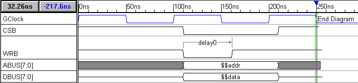
The portion of the timing diagram that contains the delay should look like this:
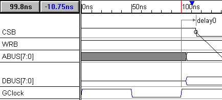
We did not enter values for the min
and max properties of
the delay because these values will be controlled from the top-level test bench.
5) Add a Continuous Setup Checker to the Read Transaction
There are two types of setups that can be created using TestBencher. The setup checker we will create
is a continuous setup. This type will verify the setup at every edge specified during the timing transaction
(every negative edge of GClock
in this case). The second type of setup, a point setup, can be added using the
setup button
 on the button bar in the Timing Diagram Editor window. This type of timing constraint verifies the timing
between two specific edges in the diagram to ensure that the signal of interest is stable for the required
amount of time.
on the button bar in the Timing Diagram Editor window. This type of timing constraint verifies the timing
between two specific edges in the diagram to ensure that the signal of interest is stable for the required
amount of time.
A continuous setup checker will be used to determine the point of failure in the test of this model.
We will specify an amount of time for which the value of DBUS must be stable before each negative edge of the global clock. Since we
are going to sweep the transition timing for the CSB signal (which controls when the read is performed),
at some point during the simulation this test will fail, providing the point of failure for the model.
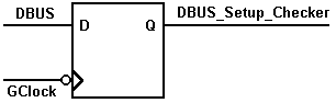
We use a flip-flop (shown below) to model the continuous setup checker. In order to create the setup
checker (the flip-flop), we will need to create a new signal. This signal will be simulated and it will
be kept internal to the diagram.
To add a continuous setup checker to the read transaction:
-
Click the Add Signal button
 on the button bar.
-
Double click the name of the new signal (SIG0) to open the Signal Properties dialog box.
-
Type DBUS_Setup_Checker in
the Name
edit box.
-
Select the Simulate radio button so that the signal will be
continuously simulated.
-
Set the
Clock to GClock and the Edge/Level to neg.
This will ensure that the continuous setup checker validates at every negative edge of the global clock.
-
Type DBUS in the Boolean Equation
edit box. This setup checker will be used to test DBUS, so that is the signal whose value we will use
in the boolean equation.
-
Set the
direction of the signal to be
internal. This will make sure that this signal is kept internal to the read component;
in this simulation, there is no reason for any other transaction to make use of it.
-
Set the
MSB value to 7 and the LSB
value to 0. In order to verify the correct value, the checker must be of the same
bus size as the signal it is testing.
-
Click the Advanced Register button to open the
Advanced Register and Latch Controls
-
Type the value 10 in the Setup edit box of this dialog. This defines the amount of
time that the signal being checked must be stable in order to prevent a failure.
-
Click OK to close the
Advanced Register and Latch Controls
dialog.
-
Click OK to close the
Signal Properties dialog.
-
Select the
File > Save Timing Diagram menu option to save the changes made to the timing diagram.
6) Examine the Write Transaction
The write transaction has already been completed for this tutorial, however we will examine the diagram
as a review of the types of changes that need to be made to a timing diagram. To open the write transaction:
-
In the Project window,
double click on the tbwrite.tim
filename.
The timing diagram will look like this:
Verify that the following statements are true:
-
The direction for GClock is
'input' which is indicated by a blue signal color. (The direction can be changed using the
Signal Properties dialog.)
-
Double click delay0 to open the Delay Properties dialog. The Is Apply Subroutine Input and the Enable HDL Code Generation
checkboxes are checked. Remember that the first checkbox makes
the min/max timing values of delay0
into inputs to the Apply call for this transaction, while the second checkbox allows the HDL code to
be generated for the delay (as described for the free parameter in Step 1).
Click OK to close the dialog.
-
Select all signals except GClock. Right click over the highlighted signal names and select Edit Selected Signal(s) from the
pop-up context menu. Make sure that the selected
Clock
is GClock
and that the Edge/Level
setting is set to pos
in the Signal Properties dialog. These settings indicate that tbwrite will generate cycle-based code.
Click OK to close the Signal
Properties dialog.
7) Applying Timing Transactions to the Template File
The Template file that generates the top-level test
bench has been partially completed and added to the project. You will need to add Apply statements that
will sequence the timing transactions. By entering the Apply statements in the template file you are
defining the execution order of the timing transactions in the final test bench.
First we will add the global clock and set it up to run continuously looping, and concurrently with
the other timing transactions. Then we will add the diagram calls for the write transaction and the
read transaction. The read and write transactions will be set to run once in a blocking mode so that
timing diagrams applied after will have to wait for the current transaction to complete.
Apply timing transactions
-
In the Project window, double click the tbench1 template file.
This will cause an editor window to open and display the template code.
-
Scroll down in the template file until you find the comment block that has this line:
Add apply calls for timing diagram transactions after this comment block:
(This comment is almost at the very end of the file.)
-
Left click in the tbench1
editor window below this comment so that the blinking cursor is in the place where you want to
add the apply statements.
-
Right click in the same place and choose Insert Diagram Calls...
from the pop-up menu to open the Insert Diagram Subroutine dialog. (If you prefer, you can
choose the Editor > Insert Diagram Calls...
main menu function.)
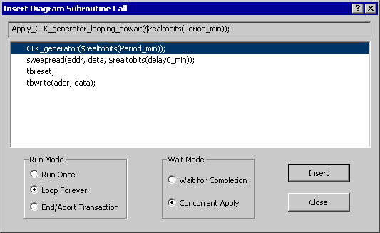
Notice that there are parameters listed in the tbread and tbwrite subroutine calls. These parameters
allow you to provide the input values for the delay min setting and bus values for the data and address
buses. The parameter in the global clock subroutine allows you to provide input values for the period
of the clock.
-
Choose the Loop Forever radio
button for the Run Mode
and the Concurrent Apply
radio button for the Wait Mode. These settings will cause the clock to run for the entire simulation,
with other transactions running concurrently.
-
Double left click the
Apply_tbglobal_clock( ... ) statement. This will place the code
for a diagram call in the template file that looks like:
For Verilog:
// Apply_tbglobal_clock_looping_nowait( $realtobits(Period_min) );
Apply_tbglobal_clock_looping_nowait( $realtobits(Period_min) );
For VHDL:
-- Apply_tbglobal_clock_looping_nowait(
tb_Control, tb_InstancePath , Period_min_real );
Apply_tbglobal_clock_looping_nowait(
tb_Control, tb_InstancePath , Period_min_real );
-
Now set the Run Mode back to Run Once and the
Wait Mode back to Wait for Completion.
-
Double left click the Apply_tbwrite(...) statement. This will add an
Apply statement for the tbwrite
transaction to your template file below the apply statement for the global clock.
-
Double left click the Apply_tbread(...) statement to add a diagram
call for the read transaction.
-
Click the Close button to close the
Insert Diagram Subroutine Call dialog.
The template file now has three diagram subroutine calls listed. We will be using a constant value for
the clock period in this simulation, so we will modify the parameters to the global clock diagram call.
-
In the tbench1 editor window, replace the two parameter names
in the global clock call with the value '100'. This will provide a period of 100ns for the clock.
// Apply_tbglobal_clock ( $realtobits(Period.min) );
Apply_tbglobal_clock( $realtobits(100.0) ); // for Verilog
Apply_tbglobal_clock( tb_Control, tb_InstancePath , 100.0 );
-- for VHDL
We will edit the read and write apply calls in the next section, when we add HDL code to the sequencer
process to generate the changing values for the delay.
8) Adding HDL Code to Sweep the Delay
The diagram subroutine calls were placed in the Sequencer portion of the test bench. The sequencer controls
the order and manner in which the timing transactions are executed. In this case, we want to add a for-loop around the diagram calls that will change the values of
the delays so that the sweep effect is created.
8.1 Add a Variable to the Sequencer
In order to create the for-loop,
we need a variable to store the current value that we are applying. This variable can then be changed
with each iteration of the for-loop.
To add the variable:
-
Locate the comment in the template code that says:
Sequencer Process
(This comment will be just a little bit above the diagram calls that
we just inserted.)
-
Insert one of the two variable declarations shown
in bold text below (the lines of text that will surround the declaration are provided for the sake of
clarity).
For Verilog (italic code is already in the file):
// Sequencer Process
real delay0; // delay0
will serve as the index and the delay value
initial
For VHDL (italic code is already in the file):
process
variable delay0 : real; -- delay0 will
hold the delay value
begin
8.2 Add a For-Loop and Input Values to the Diagram Calls
Since we have specified that the global clock will be applied continuously throughout the simulation,
we do not want to include it in the for-loop. Both the write and the read transactions will be
included in the for-loop, so that we can repeat their execution until the point of failure is found.
You may have noticed that the delays in the read and write transaction have the same name. The two delays
are completely independent of one another since they reside in different timing diagrams. TestBencher
will not try to relate the two delays. We have given the two delays the same name because (for the sake
of simplicity) we are going to provide the same input values for the two delays.
Skip to the section below for the language you are working with, then modify the sequencer code so that
it matches what is below. After that is done, we will discuss the changes that were made and what they
are doing.
Verilog Users:
Modify the template file so that it matches the following HDL code (code in italic is already present):
for (delay0 = 32.0; delay0 > 5.0; delay0 = delay0 - 5.0)
begin
// Apply_Tbwrite( addr , data , $realtobits(delay0_min)
);
Apply_Tbwrite( 'hF0 , 'hAE , $realtobits(delay0)
);
// Apply_tbread( addr , data , $realtobits(delay0_min)
);
Apply_tbread( 'hF0 , 'hAE , $realtobits(delay0));
end
VHDL '93 Users:
Modify the template file so that it matches the
following HDL code (code in italic is already present):
for i in 0 to 5 loop
delay0 := real (32 - (i * 5));
-- Apply_Tbwrite( tb_Control, tb_InstancePath , addr
, data , delay0_min_real );
Apply_Tbwrite( tb_Control, tb_InstancePath , x"F0" , x"AE"
, delay0 );
-- Apply_tbread( tb_Control, tb_InstancePath , addr
, data , delay0_min_real );
Apply_tbread( tb_Control, tb_InstancePath , x"F0" , x"AE"
, delay0 );
end loop;
VHDL '87 Users:
Modify the template file so that it matches the
following HDL code (code in italic is already present):
for i in 0 to 5 loop
delay0 := real (32 - (i * 5));
-- Apply_Tbwrite( tb_Control, tb_InstancePath , addr
, data , delay0_min_real );
Apply_Tbwrite( tb_Control, tb_InstancePath , "11110000"
, "10101110" , delay0 );
-- Apply_tbread( tb_Control, tb_InstancePath , addr
, data , delay0_min_real );
Apply_tbread( tb_Control, tb_InstancePath , "11110000"
, "10101110" , delay0 );
end loop;
Evaluating the HDL Code
The for-loop that we have entered will repeat 6 times. The input
value for the delays will be reduced by five with each iteration, producing the sweep effect. Two timing
errors will be reported. The first will be in the first loop and will be caused by the fact that the
falling edge of CSB does not set up properly before the next falling edge of the clock (this happens
because the delay is too long). The second error will be reported by the continuous setup checker during
the final iteration. This error will report a message for each bit of DBUS, for a total of eight messages.
The loop that we have created will cause the read and write transactions to iterate once for each iteration
of the loop unconditionally.
8.3 Ending the Simulation from the Test Bench
Since we have applied the global clock to run in a continuous loop, the simulation will never end unless
we manually end the execution of the global clock once the other transactions have completed. Normally
you would have to end the simulation manually through the simulator for this sort of case. We have provided
a special Abort call for each
timing transaction that you can use to end the execution of that transaction. To make use of this, add
the following line to the HDL code after the end of the for-loop:
For Verilog:
Abort_tbglobal_Clock;
For VHDL:
Abort_tbglobal_Clock(tb_Control, tb_InstancePath);
This subroutine call will end the execution of the global clock. This will ensure that the simulation
will end without the need for manual interference.
8.4 Save the Template File
Save your template file by right clicking in the template file
editor window and selecting Save from the pop-up menu.
9) Generating the Test Bench and Simulating the Project
Before simulating the project, we must generate the HDL code for the top-level test bench. To generate
this code:
-
Select the Export > Generate Test Bench
menu option. This will expand the macros in the template file, with the generated HDL code for the top-level
test bench in the file.
Simulating the Project with TestBencher's Built in Verilog Simulator
To simulate the project:
-
Click the yellow
 test bench compile button. TestBencher may ask if you want to insert signals to a new diagram at this
point. You should click Yes
so that signals are not inserted into the current diagram.
test bench compile button. TestBencher may ask if you want to insert signals to a new diagram at this
point. You should click Yes
so that signals are not inserted into the current diagram.
-
Click on the green
 simulation run button to simulate the project. This will run the simulation.
Simulating the Project Using the ModelSim Integration Feature
If you are using the ModelSim integration feature, click the yellow tb button
to autolaunch ModelSim and build the Project libraries. See Section 2.5
of the TestBencher manual (or on-line help) for more information about ModelSim integration.
Simulating the Project Using Another Third Party Simulator
The files that you will need are:
-
The HDL files for the MUT (your original model code). For this tutorial
either tbsram.v or
tbsram.vhd is the MUT
file.
-
One HDL code file for each timing transaction. These files are named
after the timing diagram names. For this tutorial you will have either tbglobal_clock.v, tbread.v
and tbwrite.v, or
tbglobal_clock.vhd, tbread.vhd and
tbwrite.vhd depending on language.
-
One top-level HDL test bench file (this is the expanded template file).
For this tutorial it is named tbench1.v
or tbench1.vhd.
-
The wavelib_inertial.v or wavelib.vhd
library file (found in the TestBencher installation directory).
-
For VHDL, there are two additional package files you must include in
your work directory: syncad.vhd
which contains generic types and tasks used by TestBencher and a project-specific package file called
tb_SweepTest1_tasks.vhd,
where SweepTest1 is the
name of the project.
This completes the Performing a Sweep Test
tutorial. During the course of this tutorial we have discussed:
-
Creating a global clock and synchronizing transaction stimulus with
the clock.
-
Creating a free parameter for use as an input to a timing transaction.
-
Creating a delay whose values are an input to the timing transaction.
-
Controlling the execution mode of a timing transaction.
-
Adding HDL code to the sequencer process of the template file.
-
Aborting a continuously executing transaction from the top-level test
bench.
Another Method of Creating a Sweep Test
An example project has been created for you to examine that demonstrates another method of performing
a sweep test. The second method uses a timing-based test bench instead of the cycle-based test bench
used in this tutorial. In the second example, edge transitions are made relative to the clock edges
using delays. The method that you choose to use will depend upon the specific model that you are testing.
|