Interactive HDL Simulation Tutorial (Tutorial 2A)
This tutorial introduces the Interactive HDL Simulation. WaveFormer, VeriLogger and TestBencher Pro
have a built-in Interactive HDL Simulator that greatly reduces the amount of time needed to draw and
update a timing diagram. Using Boolean and Registered logic equations written in VHDL, Verilog, or SynaptiCAD's
syntax you can describe signals in terms of other signals in the diagram. You will no longer have to
figure the output of a combinational circuit or calculate the critical path of a synchronous circuit
by hand. SynaptiCAD's interactive simulator will generate the HDL code using information entered into
the Logic Wizard dialog and then simulate the result. Since the simulator is interactive, changes to
input waveforms will automatically re-simulate so that your timing diagrams always reflect accurate
design data.
This feature is included in the VeriLogger and TestBencher products even though they have a built in
Verilog simulator because it makes generating test benches and timing diagrams so fast that we couldn't
hold it back. In WaveFormer, it is the backbone of the timing analysis and design features. The Interactive
simulator supports multi-bit equations and true min-max timing. This tutorial contains some examples
of equations that are supported.
This tutorial assumes that you are able to draw signals and can add delays, setups, and holds to those
signals. We recommend that beginners start with the Basic Drawing and Timing Analysis Tutorial,
tutbas1.htm, to learn the basics of timing diagram editing, before attempting this tutorial.
If you are evaluating Timing Diagrammer Pro and you would like to learn about the simulation features,
close the program and restart the evaluation version in WaveFormer Pro mode.
1) Interactive HDL Simulation
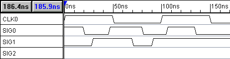
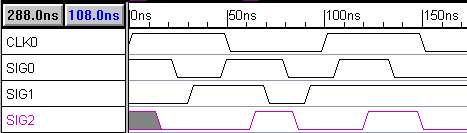
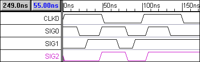
Figure 1.1: Timing diagram used for the basic HDL Simulation tutorial.
Create a timing diagram for experimenting with the Interactive HDL Simulator:
-
Add a clock named CLK0 and accept the default properties of 100ns period.
-
Add 2 signals, SIG0 and SIG1, to the timing diagram.
-
Draw the waveforms for signals SIG0 and SIG1 so that they resemble the signals in Figure
1.1. These will be the input signals for our simulation.
-
In the Parameter window, click the Add Free Parameter button
 to add a free parameter F0 to the Parameter window.
-
Double click on the free parameter F0 (in the Parameter window) to open the Parameter
Properties dialog.
-
Type 10 in the Minedit box and 15in the Maxedit box.
-
Click the OK button to close the dialog.
-
Add signal SIG2 to the timing diagram, you do not have draw the waveforms now, we will be simulating
this signal.
2) Generate Waveforms From the Boolean Equations of other Signals
We will begin by simulating a Boolean Equation. WaveFormer Pro accepts Boolean equations in either VHDL,
Verilog, or SynaptiCAD's enhanced equation syntax. The SynaptiCAD format supports the following operators:
and or &, or or |, nand, nor, xor or ^,
not or ~ or !, and delay.
The delay operator takes a signal on the left, and a time or parameter name on the right, and
returns a signal. If a parameter name is used on the right hand side of the delay operator, then the
equation will simulate true min/max timing. This true min/max timing is the main advantage that SynaptiCAD's
format has over the VHDL or Verilog format.
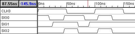
Simulate a Boolean equation:
-
Double click the SIG2 signal name to open the Signal Properties dialog. Arrange the Signal
Properties dialog so that you can see the dialog and the 3 signals at the same time. This dialog
is modeless, so leave it open for this entire section. All controls and buttons used in this section
are contained in the Signal Properties dialog.
-
Make sure that the Boolean Equation radio button
 is selected.
-
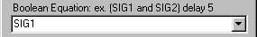
Type the following equation into the Boolean equation edit box (signal names are case sensitive): SIG0
and SIG1
-
Click the Simulate Once button and watch the signal draw itself. Notice that SIG2 is the result
of the Boolean Equation "SIG0 and SIG1". By default, the Simulate radio button is not
checked, so if you moved an edge on SIG0, SIG2 is not automatically re-simulated.
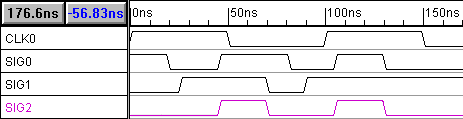
Continuously Simulate the Boolean Equation:
-
Enable the Simulate radio button. Notice that the SIG2 is now drawn in purple. This color means
that the signal is being continuously simulated, and changes in the input waveforms cause automatic
resimulations. If you are using VeriLogger Pro or TestBencher Pro, make sure that the program is in
Auto Run
 simulation mode. Debug Run mode will not continuously update signals. The Auto Run/ Debug Run simulation
mode button is located on the simulation toolbar, in the upper left of the window below the Project
menu.
simulation mode. Debug Run mode will not continuously update signals. The Auto Run/ Debug Run simulation
mode button is located on the simulation toolbar, in the upper left of the window below the Project
menu.
-
Move some of the edges on SIG0 and SIG1 and watch SIG2 re-simulate. (Notice that you cannot drag and
drop SIG2's signal edges because they are calculated edges).
3) Boolean Equations with Delays
Next we will modify the Boolean Equation to take into account the propagation delay through the AND
gate. First we simulate a simple 15ns delay, then we will simulate a min/max delay.
Simulate a simple delay:
-
Enter one of the following Verilog, VHDL, or SynaptiCAD
equations into the Boolean Equation edit box of SIG2:
#15 (SIG0 & SIG1)
(SIG0 and SIG1) after 15
(SIG0 and SIG1) delay 15
-
Click the Apply button and verify that SIG2 is correctly drawn.
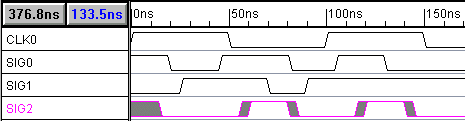
Simulate a true min/max delay using SynaptiCAD syntax:
-
Modify the Boolean Equation of SIG2 to take into account the min and max propagation delay
of the AND gate. Enter (SIG0 and SIG1) delay F0 into the Boolean Equation edit box. This
Boolean Equation references the Free Parameter F0 that you added at the beginning of the tutorial.
-
Click the Apply button to cause a simulation. Notice the gray uncertainty regions on SIG2. This
true min/max timing is the main advantage that SynaptiCAD's format has over the VHDL or Verilog format.
View the HDL code that models the Boolean equation:
-
Click the Verilog or VHDL radio button
 to view the HDL code that simulates the Boolean Equation. Native HDL code can be added here to perform
a special function. Do not modify the code now. The code should resemble the following example:
to view the HDL code that simulates the Boolean Equation. Native HDL code can be added here to perform
a special function. Do not modify the code now. The code should resemble the following example:
wire  # F0_min  SIG2_wf2 = (SIG0  & SIG1 );

wire  # F0_max  SIG2_wf3 = (SIG0  & SIG1 );

assign  SIG2 = (SIG2_wf2 === SIG2_wf3) ? SIG2_wf2 : 'bx;
-
Click the Boolean Equation radio button to display the Logic Wizard section (or Boolean Equation
Section) of the Signal Properties dialog.
-
Leave the Signal Properties dialog open. We will be using it in the next section.
Note: This example demonstrated true min/max simulation, however Min-Only and Max-Only simulations
can be performed by changing theselection inthe Timing Model drop-down list of the Simulation
Preferencesdialog box. The Simulation Preferences dialog
can be opened using the Options > Diagram Simulation Preferences menu option. The Timing Modeldrop-down list is
in the upper right corner.
4) Registered and Latched Signals
The Interactive Simulator can register or latch the result of a Boolean equation. Figure 1.2 represents
the circuit that is modeled.
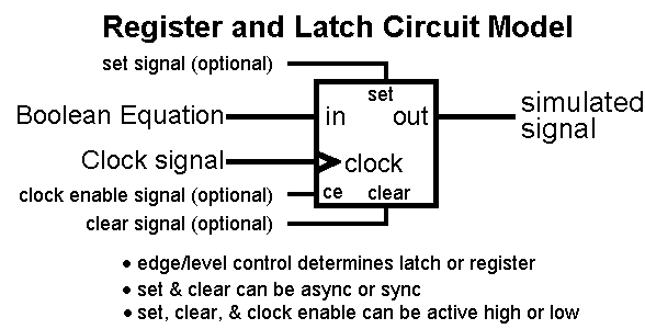
Figure 1.2:Register and Latch circuit modeled by the Logic Wizard section of the Signal Properties
dialog.
The Signal Properties dialog should still be open and displaying the SIG2 information
from the last section. Let's experiment with the register and latch functions:
-
Enter the equation SIG1 into the Boolean Equation edit box of SIG2.
-
Click the Simulate Once button to simulate the equation. SIG2 should look like an exact copy
of SIG1. When we register SIG2 you can visually compare it to SIG1 to see the effects of the register.
-
Next use the Clock drop down list box and choose SIG0 as the clocking signal.
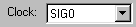 The clocking signal can be any clock or signal in the timing diagram (the default value "Unclocked"
means no flip-flop is present).
The clocking signal can be any clock or signal in the timing diagram (the default value "Unclocked"
means no flip-flop is present).
-
Next use the Edge/Level drop down list box (on the right side of the dialog) and choose both
as the triggering edge.

-
Click the Simulate Once button to simulate the circuit. Notice that SIG2 only transitions when
SIG0 has a positive or negative edge transition (move some edges on SIG0 and SIG1 to verify this).
Whether a Register or a Latch is simulated depends on the type of triggering in the Edge/Level
list box. For a Register circuit choose neg for negative edge triggering, pos for positive
edge triggering, or both for edge triggering. For a Latch circuit, choose either low or
high level latching.
-
Choose different Edge/Level values and press the Simulate Once button to verify the operation
of the register and latch functions.
5) Set and Clear Lines
The Set and Clear lines are useful when defining circuits whose initial value needs to
be specified. In this example we will demonstrate how to design a divide by 2 circuit using a
negative edge triggered register with an asynchronous active-low set line.
To specify the initial value:
-
Click the Add Signal button to create a new signal named SIG3.
-
Double click on the SIG3 name to open the Signal Propertiesdialog.
-
Type !SIG3 into the Boolean Equation edit box (it references itself in the Boolean Equation).
-
Choose CLK0 from the Clock drop down list box.
-
Make sure the Edge/Level setting is set to neg
 . .
-
Click the Simulate radio button. Notice that the waveform for SIG3 is completely gray but that
status reports Simulation Good
 (lower right corner of the window). This is because SIG3's Boolean equation references itself but it
does not provide the simulator with a known start state.
(lower right corner of the window). This is because SIG3's Boolean equation references itself but it
does not provide the simulator with a known start state.
-
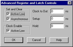
Click the Advanced Register
 button to open the Advanced Register and Latch Controlsdialog. All the register and latch individual
propagation times, setup/hold constraints, clock enable, and set/clear options are set here. Note that
Global defaults are set using the Options > Simulation Preferences menu.
button to open the Advanced Register and Latch Controlsdialog. All the register and latch individual
propagation times, setup/hold constraints, clock enable, and set/clear options are set here. Note that
Global defaults are set using the Options > Simulation Preferences menu.
-
Make sure the Active Low and the Asynchronous check boxes in the Set and Clear
section are checked. Click OK to close the dialog.
-
Choose SIG0 in the Set drop down list box
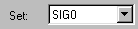 of the Signal Properties dialog.
-
Click the Simulate Once
 button. This button is located at the top left corner of the Signal Properties box, under the signal
name. Notice that SIG3 now has
a simulated waveform. Experiment with SIG0 to see how the active low set line affects the operation
of the flip-flop. You may want to redraw SIG0 so that it goes low early in the timing
diagram, and then stays high for 4 or 5 clock cycles.
button. This button is located at the top left corner of the Signal Properties box, under the signal
name. Notice that SIG3 now has
a simulated waveform. Experiment with SIG0 to see how the active low set line affects the operation
of the flip-flop. You may want to redraw SIG0 so that it goes low early in the timing
diagram, and then stays high for 4 or 5 clock cycles.
The Clock to Out, Setup, and Hold edit boxes in the Advanced Register dialog
accept time values for various timing constraints on the register and latch circuit. For more information
on Register and Latch timing read the on-line help Chapter 12: Interactive HDL Simulation.
6) Multi-bit Equations
The Interactive Simulator can automatically generate multi-bit equations for the register, latch and
combinatorial logic circuits. To convert a register or latch circuit into a multi-bit signal, change
the MSB of the input signal and the MSB of the register or latch. If the sizes of the signals do not
match, WaveFormer maps as many LSB's as it can.
First setup the diagram to experiment with multi-bit equations:
-
Delete the SIG3 signal.
-
Create a copy of SIG2. Click on the SIG2 name in the Label window to select it. Select the Edit
> Copy Signals menu option to copy the signal, then the Edit > Paste Signals option
to paste the signal. There are now two signals named SIG2 in your diagram. Rename the bottom SIG2 to
SIGX. SIGX should have the exact same waveform as SIG2.
Next, change the output of SIGX to a multi-bit signal:
-
Double click on the SIGX signal name to edit it in the Signal Properties dialog.
-
Make sure the Simulate radio button is selected.
-
Type 3 in the Bus MSB edit box. This will make SIGX a 4-bit signal.
-
Click the Apply button. SIGX's waveform is now drawn as a bus with a 4 bit binary display. Only
the LSB of SIGX is working because the input signal SIG1 is a single bit. Compare SIG2 and SIGX and
verify that they are the same values.
Change the input signal SIG1 to a multi-bit signal:
-
Double click on the SIG1 signal name to edit it the Signal Properties dialog.
-
Change the name of SIG1 to SIG1[3:0]. Changing the name using the bracket notation has
the same effect as changing the values in the MSB and LSB edit boxes.
-
Click the Apply button to accept the change. Now all four bits of SIGX should be toggling 1111
and 0000. If the radix is in Hex, the signal will toggle between 0 and F. The radix box is located
in the lower left part of the Signal Properties dialog.
If you want to further experiment with multi-bit signals, change SIG1's graphical segments to Valid
regions instead of Highs and Lows. Then double click on a valid region to open the Edit Bus State
dialog box. Type different 4-bit values, like 1010 or 0011, into the Virtual edit box and watch
how it affects the output of SIGX.
Next, setup the diagram for the next section:
-
Delete signals SIG1, SIG2, and SIGX by selecting the names and pressing the Delete
key.
-
Add a signal called SIG1. Do not draw the waveform, we will simulate it in the next section.
-
The timing diagram should consist of one clock (CLK0), and 2 signals (SIG1 and SIG0).
7) Experiment with Behavioral HDL Code
In addition to the simulation of Boolean and registered logic circuits, SynaptiCAD products can simulate
behavioral HDL code. To enter behavioral code for a signal, click oneither the Verilog or the
VHDL button in the Signal Properties dialog and type code directly into the edit box.
WaveFormer Pro, VeriLogger Pro and TestBencher Pro also provide a template feature that allows you auto
generate the register and latch models used by the Logic Wizard. In this section we will use a register
template as a starting point to build a circuit that asynchronously counts the number of edges that
occur on SIG1 and synchronously presents the total number of edges on the negative edge of the clock.
To model this circuit:
-
Double click on the SIG1 signal name to edit it in the Signal Properties dialog.
-
Choose CLK0 from the Clock drop-down list box.
-
Choose neg from the Edge/Level drop-down list box.
-
Type 3 into the Bus MSB edit box.
-
Click the Verilog code radio button to view the resulting template code:
wire [3:0] SIG1_wf1 = PLACEHOLDER;
 wire [3:0] SIG1_wf0;
 registerN_Asyn #(4,1,1) registerN_Asyn_SIG1(SIG1_wf0,CLK0,SIG1_wf1,1'b0,1'b1,1'b1,
 $realtobits(0.0),$realtobits(0.0),
 $realtobits(0.0),$realtobits(0.0));
 assign SIG1 = SIG1_wf0;
Note: the internal wire name SIG1_wf*** will vary depending on how many signals you have simulated.
The auto generated variable PLACEHOLDER is undefined and will not simulate. If a Boolean equation
was defined for the circuit, it would replace the PLACEHOLDER variable. The registerN_Asyn line
instantiates (defines an instance of) a 4 bit negative-edge-triggered register of the type used by the
logic wizard. This register takes PLACEHOLDER as an input and outputs a synchronized version on SIG1.
-
We will use the PLACEHOLDER variable to store the edge count. Edit the behavioral code so that it looks
like this (add the bold lines):
reg [3:0] PLACEHOLDER;
initial PLACEHOLDER = 0;
always @(SIG0)

PLACEHOLDER = PLACEHOLDER + 1;
wire [3:0]  SIG1_wf1 = PLACEHOLDER;
wire [3:0]  SIG1_wf0;
registerN_Asyn #(4,1,1) registerN_Asyn_SIG1(SIG1_wf0,CLK0,SIG1_wf1,1'b0,1'b1,1'b1,
  $realtobits(0.0),$realtobits(0.0),
  $realtobits(0.0),$realtobits(0.0));
assign SIG1 = SIG1_wf0;
-
Click the Simulate radio button. Verify that SIG1 is counting the edges of SIG0. The new edge count
is presented on each negative edge of CLK0.
The code that you just entered is behavioral Verilog code. The first line defines PLACEHOLDER as a 4-bit
register. PLACEHOLDER needs to be defined as a register rather than a wire in this case because it must
"remember" its value. Verilog wires don't remember their values so they must be constantly
driven to retain their value. The 2nd line initializes the value of PLACEHOLDER to 0 when the simulator
first runs. The 3rd and 4th lines contain an always block (note for VHDL users: these work like VHDL
process blocks). Whenever SIG0 changes state, the always block will execute, incrementing PLACEHOLDER.
The last 2 lines consist of the automatically generated template code that instantiates the synchronizing
register.
Tip: More information on the HDL simulator can be found in
Chapter 12: Interactive HDL Simulation in the manual and the on-line help. Also the Advanced Modeling and Interactive Simulation tutorial demonstrates
how to model a complex circuit using external models, behavioral HDL code, and incremental simulation
techniques. The HDL Simulation features are different from the VHDL and Verilog testbench generation
features which are covered in the Advanced HDL Simulation, VeriLogger Pro, and TestBencher Pro tutorials.
8) Summary
Congratulations! You have completed the Interactive HDL Simulation tutorial. In this tutorial we have
introduced the use of Boolean Equations and the beneficial features of the Boolean Equation edit box.
We examined the generation of waveforms using equations, simulation of delays, and viewing HDL code
generated from an equation. We also covered Register and Latched signals, Multi-Bit signals, and editing
behavioral code. For more information please refer to the manual or the on-line help.
|