|
|||||||||||||||||||||||||||||||||||||||||||||||||||||||||||||||||||||||||||||||||||||||||||||||||||||
|
|
Top-Down Timing Designby Brian Hoyer and Donna MitchellAppeared in Integrated System Design magazine, July 1997 Download article in Acrobat format What isTop-Down Timing Design?Generally when a design is started, a designer is given high level timing requirements that must be met by his design. Examples of high-level timing requirements include computational throughput (e.g. millions of instructions per second), data transmission rates (e.g. megabytes per second), and response latencies to requests from external systems. A designer takes these times and converts them into cycle times (for example, 10 MIPS = 100ns per instruction). These cycle times serve as "timing budgets" for the designer that he must work within during the design of his system. As the design is broken down into smaller and smaller subsystems, the cycle times are subdivided and assigned to each subsystem. The process of moving through each successive level of timing is top-down timing design. How does Top-Down Timing Design differ from Back-End Timing Analysis?The key feature of a top-down timing design methodology is an upfront analysis of system timing (usually using timing diagrams) right at the beginning of the design cycle where errors can be quickly corrected. Back-end timing analyzers such as digital simulators and static timing analyzers require the designer to have already committed to a specific circuit implementation (usually specified as a schematic or HDL netlist with associated simulations models). This requirement for a nearly completed design prior to beginning timing analysis means that any timing errors discovered during a back-end analysis may result in a significant redesign effort. In addition, when timing or logic errors are found at this stage, any circuit changes must be reflected in many different places: the schematic, model descriptions, test bench stimulus for the simulator or timing analyzer, and documentation accompanying the design. Top-down timing design helps the designer discover timing errors earlier in the design cycle, resulting in fewer changes and faster product development. Back-end timing analyzers are most useful as design sign-off validators rather than as design aids. It is difficult to use a back-end timing analyzer to maximize design speed because most of the design decisions have been made by the time a back-end timing analysis begins. Examination of significantly different design choices is not possible because each design alternative requires too much front-end design time before its performance can be analyzed. Front-end timing analyzers such as WaveFormer Pro by SynaptiCAD Inc. (see Figure 1), excel at timing optimization because comparatively little design information needs to be entered in order to analyze system performance. Front end timing analyzers don't invalidate the use of back-end timing analyzers. While front end timing analyzers are quicker and require less design entry, back-end timing analyzers benefit from having complete design information and generally perform a more exhaustive, brute force analysis of a design's performance that can detect errors that a designer may have neglected to check for during a front-end timing analysis. In fact, one of the biggest challenges of using a back-end timing analyzer is sifting through the data generated by the analysis to discover real timing errors. Nonetheless, the additional security provided by a back-end timing analysis prior to design sign-off argues for the combined use of a front and back-end timing analyzer when using a top-down design approach. Benefits of timing diagram analysisDesigner's have traditionally used hand-drawn timing diagrams to perform their initial timing analysis. Timing diagrams offer the advantage of being able to see the effects of timing constraints on a system's signals. With a timing diagram, the cause-effect relationships between signal transitions are shown by timing parameters such as delays, setups, and holds, providing a designer with more insight into the operation of a system. This is particularly helpful because timing errors are found early in the design cycle. Also critical paths that cause errors can be analyzed visually by following delay chains back through the diagram. Each delay in a critical path suggests a point at which a circuit change could alleviate a timing error or increase system performance.
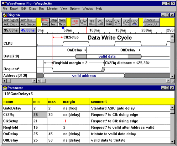
Figure 1. Timing diagram used for top down timing design. The screeen capture of WaveFormer Pro shows margin calculations and delay parameters. Timing diagram analysis also gives you the advantage of being able to account for min/max delay tolerances at the same time. This is critical for asynchronous designs such as bus transaction protocols because most simulators can only simulate at the extreme timing end points, but not over the entire operational range of the design. Many designs are never given a thorough timing diagram analysis, despite the benefits, because of the amount of time required to perform such an analysis manually. Drawing timing diagrams by hand is a difficult and error prone task and the resulting diagrams are generally messy and hard to understand and analyze. The messiness is compounded when timing errors are discovered and fixed causing the hand drawn timing diagrams to be erased and redrawn. In addition, the timing analysis of manually generated timing diagrams is usually overly pessimistic because it is difficult to find and remove common delays from setup and hold calculations. Timing diagram editors such as WaveFormer eliminate the need to manually generate timing diagrams, making it easy to create and change timing diagrams and reducing the chance for error in timing calculations. Timing diagrams can be created with a combination of point-and-click drawing, Boolean and temporal equations, and auto-generated clocks and busses. Designers can analyze system performance using just the timing parameter information available in data books without the need for schematic netlists and complex simulation models. Timing calculations are performed interactively, so it is easy to quickly assess the impact of a change in a timing parameter by updating the parameter's value or switching to a different part library. Timing diagram editors can provide several types of timing and logic analysis:
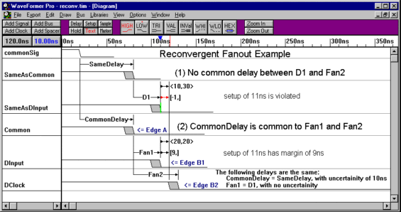
Calculation of Critical Paths and Constraint CheckingTiming calculations in a timing diagram analyzer are performed using true min/max timing, and calculations are automatically adjusted to account for subtle timing effects such as reconvergent fanout. With timing diagram editor output, it is easier to see timing relationships between signal transitions than with a simulator, because the timing parameters (propagation delays, setup times, and hold times) graphically specify cause/effect relationships between signal transitions and timing constraints that must be met by the system. This is one reason engineers still draw timing diagrams by hand even when they have access to powerful simulators. Timing diagram editors also allow designers to verify min-max timing simultaneously so that the overall impact of IC timing tolerances on a system.s performance can be properly assessed. Reconvergent FanoutMargin calculations in some circuits can be overly pessimistic if all the uncertainty times in a timing path are included in the calculations. For instance, if two signal transitions B1 and B2 are caused by the same transition A (see Figure 2), then margin calculations between B1 and B2 should not include the uncertainty of transition A, because no matter when A transitions it will occur at the same time for both B1 and B2. When this happens the circuit is said to have reconvergent fanout, because this typically occurs when two signals diverge (fanout) from a common source and reconverge at the inputs of a gate. The adjustment of timing calculations to account for reconvergent fanout is referred to as common delay removal, because the uncertainty created by delays common to both timing paths is removed. The ability to recognize and remove the pessimistic effects of reconvergent fanout is especially important for circuits with demanding timing requirements. Performing common delay removal on manually drawn timing diagrams is tedious and error prone, but ignoring this effect can lead to sub-optimal designs.
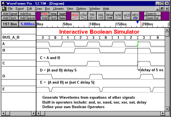
Figure 2. Reconvergent fanout example. Reconvergent fanout adjustment removes common delays from calculation margin and distance values. Delay CorrelationAnother effect that is rarely accounted for in digital designs that can lead to overly pessimistic margin calculations is delay correlation. Delay correlation allows the designer to specify that the degree of variation in gate delays on a single chip is smaller than the variation of gate delays across multiple chips. This lower variation in on-chip delays makes it possible for designs to meet setup and hold time requirements that could not be met using just the min/max delay values. Delay correlation is expressed as a percentage value. By default, delays in WaveFormer Pro are considered uncorrelated (delay correlation = 0%). 100% delay correlation between a group of gates would mean that all the gates are guaranteed to have exactly the same propagation delay time. Note that this delay time could be anywhere between the min and max time of the delay parameter, but whatever the value it would be the same of all the gates. For example, two gates with a min/max delay = 5-15 ns and a correlation of 90% could have delay values anywhere in the range between 5 and 15 nanoseconds, but the delays of the gates are guaranteed to be within 1 nanosecond ( (15ns - 5ns)*90% = 1ns) of each other. Process and temperature variations across ICs account for the increased variation in across-chip gate delays. IC manufacturers do not generally publish delay correlation values for most standard TTL and CMOS parts, but they do publish delay correlation values for clock buffer ICs (correlation between clock delays is more important than absolute delay for clock trees as uncorrelated delays increase clock skew). Clock buffer delay correlation is usually specified indirectly as a min/max delay and an on-chip delay variation often called skew (e.g clock buffer with delay = 5-10 ns and on-chip skew = 1ns has a delay correlation of 80% ( 100% - 1ns / (10ns - 5ns) = 80%). Designers using ASICs and FPGAs will benefit the most from taking advantage of delay correlation in their designs, since most of the delays in these designs are correlated. If your gate array or FPGA manufacturer doesn.t publish this information in their data books, you should ask your manufacturer directly as they probably have the information available internally. The primary reason delay correlation information hasn.t been published much in the past has been the lack of EDA tools that can take advantage of it. Correlation factors in WaveFormer Pro are specified by first creating a correlation group name and assigning it a correlation percentage. Next all the correlated delays (e.g. all the delays on the chip) are added to the correlation group. For gate array designers, WaveFormer Pro supports a default correlation group which applies to all delays in a design. After delay correlations are specified WaveFormer Pro automatically adjusts all timing margins in a design. Combinatorial Logic AnalysisEarly in the top-down design cycle, after the original timing interface has been analyzed, different parts of the circuit will start to take shape. WaveFormer Pro helps you in this phase by supporting interactive Boolean simulation (see Figure 3). Designers can enter Boolean equations that describe their design and immediately assess the impact of modifying logic, state, and timing information without having to change a schematic or create simulation models. The Boolean simulator includes support for propagation and interconnect delays allowing any combinatorial logic to be modeled. Below is an example of a Boolean equation that models an AND gate with an input delay of 20ns on one input and 10ns on the other input: SIG3 = (SIG0 delay 20ns) and (SIG1 delay 10ns)
Figure 3. Interactive Boolean simulator example. Interactive Boolean simulation aids in top-down timing analysis. Temporal equations for describing DSP waveforms
Many waveforms are difficult to draw and work with because of the precise edge placement necessary to
convey circuit information. For instance, a waveform that alternates between a frequency of 25MHz and
50Mhz for 10 cycles would be very tedious to attempt to draw by hand. These types of waveforms can be
described in WaveFormer Pro using temporal equations. The waveform described above could be generated
using the following temporal equation:
Reuse timing diagrams during SimulationWaveFormer Pro can be used as a stand-alone design verification tool or in conjunction with a digital simulator. All simulators need input stimulus to perform a simulation. With WaveFormer Pro, waveform data can be saved to different simulator formats for driving simulations (e.g. VHDL, Verilog, Spice, Mentor's Quick Sim II, Viewlogic, OrCAD, Model Tech V-System, and Accolade PeakVHDL formats). In addition, WaveFormer Pro supports the import of waveforms from other tools, so it can serve as a translator between different waveform formats. WaveFormer Pro uses a scripting language based on Perl (Practical Extraction and Report Language) to import and export waveform stimulus. The use of a scripting language means users can modify the output of existing translation scripts and even create their own scripts to support waveform formats used by custom test equipment and internally developed software. SummaryTop down design is the process of starting from a high-level specification of a system and moving down through successive level of detail until a design is completed. Top down timing analysis is a natural design paradigm which fits well with interface specifications and component information taken from data books. Top-down timing analysis is difficult and error prone when performed using manually generated timing diagrams, but timing diagram editors such as SynaptiCAD's WaveFormer Pro make timing diagram analysis a rapid and relatively painless process. Timing diagram editors allows the generation of detailed timing diagrams that are vastly easier to create and maintain than those that can be generated using conventional drawing packages. Rapid design entry and rapid feedback on system functionality makes timing diagram software ideal tool for the iterative process of designing digital circuits and examining design tradeoffs in a "what-if" fashion. Some useful analysis features of timing diagram editors can include: Boolean equation simulation, critical path analysis, setup/hold margin calculation, removal of common delays from margin calculations (reconvergent fanout analysis), and timing adjustment for delay correlation. Top-down timing analysis using a timing diagram editor provides benefits throughout the design process. As a system specification and analysis tool, a timing diagram editor is particularly useful for pre-schematic analysis before simulation is possible. During the design phase a timing diagram editor can serve in a dual role as timing analyzer and test bench generator for simulations. During the documentation phase of a design, the timing diagrams generated during the top-down design process serve as a useful adjunct to schematics and other design documentation.
Bryan Hoyer is president of Boulder Creek Engineering, Saratoga CA, the makers of the Pod-A-Lyzer.
He has over 20 years of experience designing digital and analog systems. |
|
|